- 您现在的位置:买卖IC网 > Sheet目录2002 > ISLA214S50IR1Z (Intersil)IC ADC
ISLA214S50
17
FN7973.2
April 25, 2013
Analog Input
A single fully differential input (VINP/VINN) connects to the
sample and hold amplifier (SHA) of each unit ADC. The ideal
full-scale input voltage is 2.0V, centered at the VCM voltage as
shown in Figure 33.
Best performance is obtained when the analog inputs are driven
differentially. The common-mode output voltage, VCM, should be
used to properly bias the inputs as shown in Figures 34 through
36. An RF transformer will give the best noise and distortion
performance for wideband and/or high intermediate frequency
(IF) inputs. Two different transformer input schemes are shown in
This dual transformer scheme is used to improve common-mode
rejection, which keeps the common-mode level of the input
matched to VCM. The value of the shunt resistor should be
determined based on the desired load impedance. The
differential input resistance of the ISLA214S50 is 600
Ω.
The SHA design uses a switched capacitor input stage (see
Figure 48), which creates current spikes when the sampling
capacitance is reconnected to the input voltage. This causes a
disturbance at the input which must settle before the next
sampling point. Lower source impedance will result in faster
settling and improved performance. Therefore a 2:1 or 1:1
transformer and low shunt resistance are recommended for
optimal performance.
A differential amplifier, as shown in the simplified block diagram
in Figure 36, can be used in applications that require
DC-coupling. In this configuration, the amplifier will typically
dominate the achievable SNR and distortion performance.
Intersil’s new ISL552xx differential amplifier family can also be
FIGURE 32. TYPICAL SNR AND SFDR PERFORMANCE vs TEMPERATURE, DEVICE CALIBRATED AT +85°C, fIN = 105MHz
Temperature Calibration (Continued)
0
10
20
30
40
50
60
70
80
90
100
65
70
75
80
85
TEMPERATURE (°C)
S
N
R
(dBFS)
AND
S
F
DR
(dBc)
SFDR AT 500MSPS
SFDR AT 350MSPS
SNR AT 500MSPS
SNR AT 350MSPS
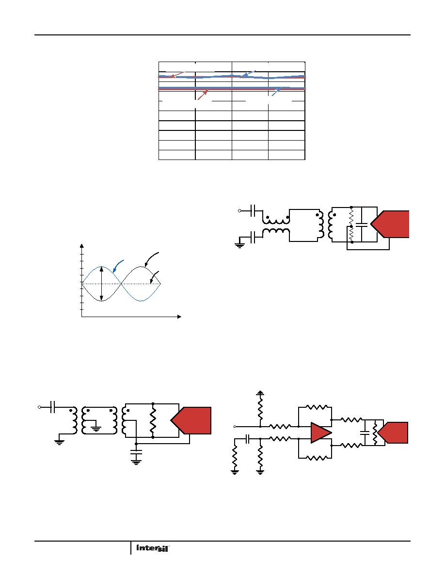
FIGURE 33. ANALOG INPUT RANGE
1.0
1.8
0.6
0.2
1.4
VINP
VINN
VCM
1.0V
FIGURE 34. TRANSFORMER INPUT FOR GENERAL PURPOSE
APPLICATIONS
ADT1-1WT
0.1F
ADC
VCM
ADT1-1WT
1000pF
FIGURE 35. TRANSMISSION-LINE TRANSFORMER INPUT FOR
HIGH IF APPLICATIONS
ADC
VCM
1000pF
TX-2-5-1
ADTL1-12
FIGURE 36. DIFFERENTIAL AMPLIFIER INPUT
ADC
发布紧急采购,3分钟左右您将得到回复。
相关PDF资料
ISLA222P13IRZ
IC ADC 12BIT SRL/SPI 72QFN
ISLA224S25IR1Z
IC ADC
KAD2708C-27Q68
IC ADC 8BIT 275MSPS PAR 68-QFN
KAD2708L-27Q68
IC ADC 8BIT 275MSPS PAR 68-QFN
KAD2710C-27Q68
IC ADC 10BIT 275MSPS PAR 68-QFN
KAD2710L-21Q68
IC ADC 10BIT 210MSPS SGL 68-QFN
KAD5510P-25Q48
IC ADC 10BIT CMOS 250MSPS 48QFN
KAD5510P-50Q72
IC ADC 10BIT 500MSPS SGL 72-QFN
相关代理商/技术参数
ISLA214S50IR48EV1Z
制造商:Intersil Corporation 功能描述:ISLA214S50IRZ EVALUATION BOARD 1 48LD QFN ROHS COMPLIANT - Bulk 制造商:Intersil Corporation 功能描述:ISLA214S50IRZ EVALUATION BOARD 1 48LD QFN ROHS COMPLIANT
ISLA216IR72EV1Z
制造商:Intersil Corporation 功能描述:ISLA216IR72 EVAL BOARD - 72 LD QFN - SINGLE 16-BIT 250MSPS U - Bulk 制造商:Intersil Corporation 功能描述:EVAL BOARD FOR ISLA216IR72 制造商:Intersil Corporation 功能描述:EVAL BOARD ADC ISLA216P 制造商:Intersil Corporation 功能描述:EVAL BOARD, ADC, ISLA216P 制造商:Intersil 功能描述:ISLA216IR72 EVALRD 72LD SNGL 16-BIT 制造商:Intersil Corporation 功能描述:EVAL BOARD, ADC, ISLA216P; Silicon Manufacturer:Intersil; Silicon Core Number:ISLA216P; Kit Application Type:Data Converter; Application Sub Type:ADC; Kit Contents:Evaluation Board for ISLA216P ADC
ISLA216P
制造商:INTERSIL 制造商全称:Intersil Corporation 功能描述:16-Bit, 250MSPS/200MSPS/130MSPS ADC
ISLA216P_1104
制造商:INTERSIL 制造商全称:Intersil Corporation 功能描述:16-Bit, 250MSPS/200MSPS/130MSPS ADC
ISLA216P13
制造商:INTERSIL 制造商全称:Intersil Corporation 功能描述:12-Bit, 500MSPS ADC Programmable Built-in Test Patterns
ISLA216P13IRZ
制造商:Intersil Corporation 功能描述:16-BIT 130MSPS ADC UNBUFFERED INPUT, 72-PIN QFN - Trays 制造商:Intersil Corporation 功能描述:IC ADC 16BIT SPI 130MSPS 72QFN 制造商:Intersil 功能描述:16-BIT 130MSPS ADC UNBUFRD INPUT 72-PIN 制造商:Intersil Corporation 功能描述:IC, ADC, 16BIT; Resolution (Bits):16bit; Sampling Rate:130MSPS; Supply Voltage Type:Single; Supply Voltage Min:1.7V; Supply Voltage Max:1.9V; Supply Current:293mA; Digital IC Case Style:QFN; No. of Pins:72; Data Interface:SPI ;RoHS Compliant: Yes
ISLA216P20
制造商:INTERSIL 制造商全称:Intersil Corporation 功能描述:12-Bit, 500MSPS ADC Programmable Built-in Test Patterns
ISLA216P20IRZ
制造商:Intersil Corporation 功能描述:16-BIT 200MSPS ADC UNBUFFERED INPUT, 72-PIN QFN - Trays 制造商:Intersil Corporation 功能描述:IC ADC 16BIT SPI 200MSPS 72QFN 制造商:Intersil 功能描述:16-BIT 200MSPS ADC UNBUFRD INPUT 72-PIN 制造商:Intersil Corporation 功能描述:IC, ADC, 16BIT; Resolution (Bits):16bit; Sampling Rate:200MSPS; Supply Voltage Type:Single; Supply Voltage Min:1.7V; Supply Voltage Max:1.9V; Supply Current:342mA; Digital IC Case Style:QFN; No. of Pins:72; Data Interface:SPI ;RoHS Compliant: Yes